The chip achieves speeds of 200 Gb/s thanks to slow-speed light
Executive Briefing
Synthesized and verified with gemini-2.0-flash-thinking-exp
“# The chip achieves speeds of 200 Gb/s thanks to slow-speed lighting Reduced-DSP 200G/λ developed b”
Key Takeaways
- 1.# The chip achieves speeds of 200 Gb/s thanks to slow-speed lighting Reduced-DSP 200G/λ developed by Japan, uses slow-moving light and power balance to increase data transmission speed.
- 2.According to Professor Toshihiko Baba at Yokohama National University, who leads the research team, Reduced-DSP 200G/λ has a compact size but is capable of transmitting data at speeds of up to 200 Gb/s.
- 3.The system uses slow-motion lighting and a built-in power equalizer, helping to overcome speed limitations that have plagued similar devices.
Reduced-DSP 200G/λ developed by Japan, uses slow-moving light and power balance to increase data transmission speed.
According to Professor Toshihiko Baba at Yokohama National University, who leads the research team, Reduced-DSP 200G/λ has a compact size but is capable of transmitting data at speeds of up to 200 Gb/s. The system uses slow-motion lighting and a built-in power equalizer, helping to overcome speed limitations that have plagued similar devices.
A modulator is a system used to encode information such as sound, images or digital data onto a carrier wave for transmission over cable, fiber optics or space, according to Analog Device. In optical communications, modulators control light for data transmission, contributing to increased connection speeds between devices and servers.
Silicon modulators that convert electrical signals into light are typically a few millimeters in size. However, their operability comes at a "trade-off" between modulation efficiency and high-frequency performance: slowing down the light enhances interaction with the device and improves efficiency, but resistors can limit the modulator's response speed.
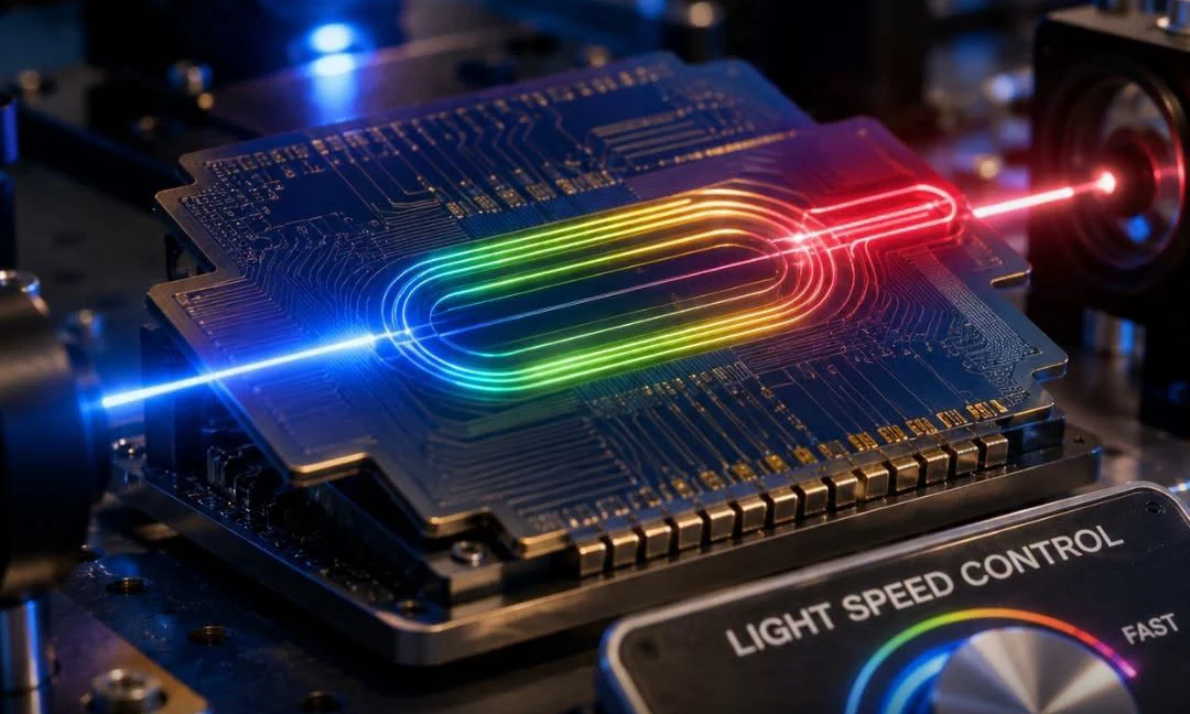
Reduced-DSP 200G/λ solves the two problems mentioned above. In a paper published in the journal Nature Communications last week, the team combined the use of optical crystal waveguides - small structures that guide light through a silicon chip, inside containing a series of carefully arranged small holes and controlling how light propagates through the material, allowing light to propagate more slowly than conventional waveguides. According to Baba, the effect increases the interaction between the light and the device, allowing a small electrical variation to produce a larger change in the light output signal. The result is the chip's ability to modulate effectively in a smaller space.
Conventional light modulators have difficulty processing signals at high speeds because resistance limits response. To fix this, the team integrates an Electro-Optical Equalizer (EO) that adjusts the combination of components of the light signal, helping the device process the signal faster while maintaining performance. Thanks to this improvement, the operating frequency range the device can handle increases from 35 to 80 GHz.
The chip is fabricated with a length of 320 µm (0.32 mm), including the main part and the balance part, lower than the 2-4 mm of today's popular silicon Mach-Zehnder modulators. The entire chip, including electrodes, occupies an area of about 0.4 square millimeters.
Despite its compactness, the new chip achieves speeds of 140 Gb/s using on-off keying, and up to 180 Gb/s using four-level pulse amplitude modulation (PAM-4) without the need for a digital signal processor (DSP). When adding an 11-tap receiver, the speed increases to 200 Gb/s.
"The great thing is that slow light can be fabricated using a CMOS compatible process, while meeting the requirements of high speed, low power consumption and compact size that bring many benefits to systems inside AI data centers," Baba said.
Despite its potential, the research team believes that the chip still has many challenges that need to be resolved. The new design helps data centers increase optical connection density, reducing energy consumption, but optical insertion loss - the reduction in light intensity when transmitted through the device - is still at 11.7-15.5 dB, much higher than silicon photonic modulators for data centers, which are at 5-7 dB.
Baba said the team worked around it with an optical amplifier to compensate, but the scope remained in the lab. Additionally, the researchers are planning to expand the range of wavelengths the modulator can handle, potentially allowing multiple optical channels to work together. The ultimate goal is to integrate 16-32 channels operating at the same time, for a combined capacity transmission speed of 3.2-6.4 Tbps.
"We believe the architecture has the potential to be the foundation for integrated optical devices for high-performance data centers in the future," Baba told Interesting Engineering.
Bao Lam summary
- The helium crisis surrounds the chip and semiconductor industry
- Why do technology companies make their own AI chips?
- Musk criticized memory chip companies for 'price gouging', but praised Micron
- AI model designs and improves semiconductor chips by itself