What does a phone camera use to take pictures: CMOS sensor turns light into electrical charge
Executive Briefing
Synthesized and verified with gemini-2.0-flash-thinking-exp
“Every time you press the shutter button on your phone, light passes through a tiny lens cluster and”
Key Takeaways
- 1.Every time you press the shutter button on your phone, light passes through a tiny lens cluster and falls onto a small silicon chip.
- 2.That chip is a CMOS image sensor, where millions of pixels simultaneously count how much light they receive.
- 3.This type of sensor is also in webcams, dash cams and most cameras today.
Every time you press the shutter button on your phone, light passes through a tiny lens cluster and falls onto a small silicon chip. That chip is a CMOS image sensor, where millions of pixels simultaneously count how much light they receive. This type of sensor is also in webcams, dash cams and most cameras today.
Light into electrons
The basic principle is the photoelectric effect that Albert Einstein explained and received the Nobel Prize in 1921: when a photon of light hits silicon, it can knock electrons out of the bond. Each pixel on the sensor contains a photodiode, an area of silicon designed to collect those electrons during exposure. Wherever it is brighter, the pixel there collects more electrons. The circuit then reads the electrical charge of each pixel, converts it into a number, and the processor puts it all together into an image.
The first successful digital sensor was the CCD, invented by Willard Boyle and George Smith at Bell Labs in 1969, a work that helped them receive the 2009 Nobel Prize in Physics. The CCD transfers charge from one pixel to another to a single output, providing good quality but consuming electricity and requiring many external auxiliary chips.
Compare two CMOS sensors: a 35mm full-frame type in the camera body and a small sensor mounted on the camera board. Phone sensors are in the small size group
From spaceship to phone
The idea of placing an amplifier right in each pixel, called an active pixel sensor (APS), was proposed by Peter Noble in 1966. In 1985, Tsutomu Nakamura's group at Olympus created the first APS sensor using MOS technology. The turning point came in the early 1990s, when Eric Fossum at NASA's Jet Propulsion Laboratory (JPL) sought to miniaturize spacecraft cameras.
Fossum's team uses the same CMOS process to produce microprocessors and memory chips to make sensors, then integrates almost every circuit of the camera, from control, analog-to-digital conversion to signal processing, onto the same chip. NASA calls it a camera on a chip. According to NASA Spinoff, this method consumes up to 100 times less electricity than CCD and is cheaper to produce. In 1995, Fossum and his colleagues founded the company Photobit to commercialize the technology, which was later acquired by Micron.
When camera phones exploded in the mid-2000s, CMOS proved suitable: small, cheap, low battery consumption. In 2007, CMOS sensor sales exceeded CCD with 54% of the market, up to 74% in 2012 and 89% in 2017. The videography industry also switched to CMOS when HD video was born, because CCDs with a large number of pixels will be hot and consume electricity.
Color comes from a filter
Photodiode only measures brightness, regardless of color. To get a color image, above each pixel is covered with a red, green or blue filter cell according to the Bayer filter, named after Kodak engineer Bryce Bayer, patented in 1976. Half of the cells are green, because the human eye is most sensitive to this color area when sensing brightness, while red and blue each make up a quarter. Because each pixel can only record one color, the software must interpolate the remaining two colors from surrounding pixels, a process called demosaicing.
Diagram illustrating the Bayer color filter and front-illuminated versus back-illuminated (BSI) pixel cross-section
Flip the chip
In traditional sensors, layers of metal wires lie between the lens and photodiode, blocking out some of the light. The smaller the pixel, the more significant the hidden portion. Back-side illumination (BSI) sensors are solved by turning the silicon sheet over when manufactured, thinning the back side so that light goes directly into the photodiode without having to go through the wire layer. According to Wikipedia, this method increases the percentage of photons captured from about 60% to more than 90%.
Advertisement
BSI technology was only used for astronomy cameras or security cameras because it was difficult and expensive to make. In 2008, OmniVision announced the 8-megapixel OV8810 BSI sensor with 1.4-micrometer-wide pixels. In August 2009, Sony brought the Exmor R series to the mass market, and the BSI sensor became the highlight of the iPhone 4 camera in 2010. In 2012, Sony went a step further with a stacked sensor, placing the processing circuit in a separate layer behind the pixel layer.
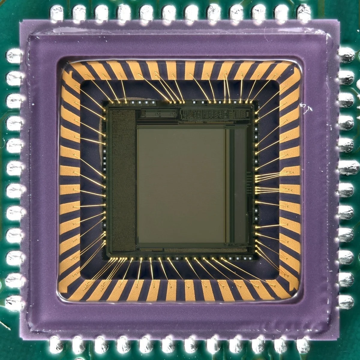
OmniVision OV7120 CMOS sensor (640 x 480 pixels) close-up view. The dark rectangular area in the middle is the pixel matrix, surrounded by the processing circuit and gold wires
Therefore, when comparing phone cameras, the number of megapixels is only a part. Sensor size, pixel size, backlighting or stacking type, and image processing software all contribute to deciding how the image turns out, especially when shooting in low light.
Source:
Wikipedia: Active-pixel sensor
,
NASA Spinoff
,
NobelPrize.org
,
Wikipedia: Bayer filter
,
Wikipedia: Back-illuminated sensor