Semiconductors: why silicon, found in sand, dominates the chip industry
Executive Briefing
Synthesized and verified with gemini-2.0-flash-thinking-exp
“Every phone or laptop contains billions of transistors engraved on thin slices of silicon.”
Key Takeaways
- 1.Every phone or laptop contains billions of transistors engraved on thin slices of silicon.
- 2.Silicon is a semiconductor, a material that is less conductive than metal but better than an insulator, and most importantly, its conductivity can be controlled.
- 3.The first transistor wasn't even made of silicon.
Every phone or laptop contains billions of transistors engraved on thin slices of silicon. Silicon is a semiconductor, a material that is less conductive than metal but better than an insulator, and most importantly, its conductivity can be controlled. The first transistor wasn't even made of silicon. Silicon wins thanks to physics, chemistry and cost.
Not quite conductive, not quite insulating
In metals like copper, there are many free electrons so electricity flows easily. In insulators like glass, electrons are tightly held around atoms. Semiconductors lie in the middle: when pure, they conduct electricity poorly, but just adding heat, light or a very small amount of foreign elements causes the conductivity to change completely.
Silicon atoms have 4 electrons in the outer shell and are bonded to 4 neighboring atoms into a regular crystal lattice. If a very small number of silicon atoms are replaced with phosphorus, which has 5 electrons, the fifth electron is extra and free to move, forming an n-type semiconductor. If replaced with boron, there are only 3 electrons, the crystal lattice is missing an electron in that place. This vacancy is called a hole, which acts as a positive charge, forming a p-type semiconductor. According to Wikipedia, the ratio of just 1 impurity atom per 100 million silicon atoms is enough to significantly increase electrical conductivity.
Diagram illustrating silicon doping: adding phosphorus to create excess electrons (n-type), adding boron to create holes (p-type)
When the p region and n region are close to each other, the p-n junction only allows current to flow easily in one direction. This is the basis of diodes, transistors and solar cells.
Germanium goes first
The first transistor was made of germanium by John Bardeen and Walter Brattain at Bell Labs in 1947. According to the Computer History Museum (USA), germanium is easier to process than silicon, but germanium transistors have large electrical leakage in the off state, which is taboo for computer logic circuits, and only runs well in the range of 0 to 70 °C. Silicone components operate from -55 to 125 °C, requiring much purer materials.
In January 1954, chemist Morris Tanenbaum at Bell Labs made the first silicon transistor, but Bell Labs did not pursue this direction. On May 10, 1954, Gordon Teal, who had left Bell Labs for Texas Instruments, caused a stir at a conference when he announced that the silicon transistor had been produced and sold. By the late 1950s, silicon had become the industry's preferred semiconductor material.
Precious oxide layer
Silicon's biggest advantage lies in its oxide layer. In 1955, Carl Frosch and Lincoln Derick at Bell Labs accidentally discovered that it was possible to grow a layer of silicon dioxide (SiO2), the same composition as quartz, right on the silicon surface. This layer is strong, insulates well and is insoluble in water. Germanium oxide is unstable, and according to Wikipedia, this is the main reason germanium-based technology fails.
In 1959, Jean Hoerni at Fairchild Semiconductor left the oxide layer intact to shield the p-n junctions, instead of removing it as was common practice at the time. His planar process creates flat, durable transistors with much less leakage. Also in 1959, Robert Noyce based on this process to patent a monolithic integrated circuit on silicon, a more practical direction than Jack Kilby's circuit which was made on germanium.
Cheap, plentiful and pure to the nines
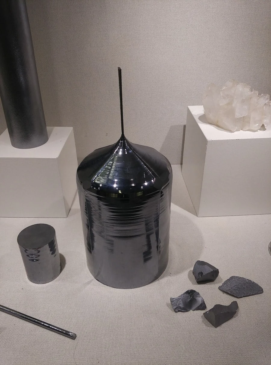
Silicon makes up about 28% of the Earth's crust, second only to oxygen, and is available in sand and quartz. Germanium is only 50th in popularity. In 1998, silicon cost less than $10 per kilogram, while germanium was nearly $800. However, the silicon used to make chips must reach a purity of 99.9999999%, often called nine nines. It is melted and spun into a single crystal ingot using the Czochralski method, then cut into round wafers up to 300 mm in diameter. Silicon also conducts heat well, about 3 times more than gallium arsenide (GaAs), so it can withstand dense transistor density.
Advertisement
Single crystal silicon ingot on display at the Munich Museum of Mineralogy (Germany). Such ingots are cut into wafers
The silicon wafer has engraved circuits, each small square is a chip. Rainbow colors are caused by microscopic circuit structures diffracting light
Silicon doesn't win everywhere
GaAs is the second most popular semiconductor after silicon. It allows electrons to run faster and emit light effectively, so it is used in laser diodes, solar cells and high-frequency microwave circuits. Supercomputer company Cray once bet on GaAs processors, but could only build one Cray-3 machine and then went bankrupt in 1995. GaAs does not have a natural oxide layer as good as silicon and is worse at conducting holes, so it is difficult to make power-saving CMOS circuits.
Therefore, silicon still serves as the main material for processors and memory, while other semiconductors take care of specialized tasks such as light emission, high-frequency waves or large voltages. The period from the late 20th century to the present is therefore also called the Silicon Age, similar to the Bronze or Iron Age.
Source:
Wikipedia: Semiconductor
,
Wikipedia: Silicon
,
Computer History Museum: Silicon transistors 1954
,
Computer History Museum: Planar process 1959
,
Wikipedia: Germanium
,
Wikipedia: Gallium arsenide
Advertisement